De los micrómetros a los picómetros: evolución de las técnicas de microscopía para el estudio de nanomateriales
Resumen
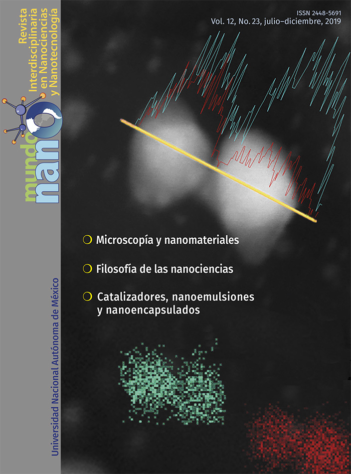
Sin lugar a duda, las técnicas de microscopía electrónica (ME) y microscopía de sonda de barrido (SPM) han contribuido enormemente al estudio de nanomateriales, dando información de propiedades morfológicas, estructurales, de superficie, eléctricas y magnéticas, entre muchas otras. Las técnicas más empleadas para estudios a nanoescala han sido las microscopías electrónicas de transmisión y barrido, y por otro lado, las de efecto túnel y de fuerza atómica, respectivamente. Los avances tecnológicos en los últimos años de estas técnicas han permitido límites de resolución que hace 25 años era inimaginables, siendo los últimos valores alcanzados de decenas de picómetros (10-12 m). Cabe señalar, que más allá de esto, las técnicas de microscopia mencionadas han crecido en sus capacidades de análisis en el campo de las nanociencias y nanotecnología, dando lugar a otras técnicas como microscopía electrónica de barrido por transmisión (STEM, del inglés Scanning Transmission Electron Microscopy), Imagen en campo obscuro a ángulo grande en alta resolución (HR-HAADF, del inglés High Resolution - High Angle Annular Dark Field), Crio-Microscopía Electrónica, Tomografía electrónica, Espectroscopía de tunelamiento, Tunelamiento inelástico, Curvas de fuerza, etc. Lo anterior, no solo ha complementado la información morfológica y estructural, sino que también, ha contribuido al entendimiento de fenómenos de interacción y propiedades fisicoquímicas a escalas atómicas y moleculares. En este artículo se hace un análisis de la trascendencia actual que tienen las técnicas de microscopía electrónica, así como las de microscopia de sonda de barrido (SPM), y se menciona brevemente el alcance de estas técnicas como métodos de modificación de superficies a ultra alta resolución, como el caso de la nanolitografía y nanomanipulación, que estan abriendo un panorama enorme en el desarrollo de las tecnologías del futuro.
Citas
Angeloni, L., Passeri, D., Corsetti, S., Peddis, D., Mantovani, D. y Rossi, M. (2017). Single nanoparticles magnetization curves by controlled tip magnetization magnetic force microscopy. Nanoscale, 9(45): 18000-18011. http://dx.doi.org/10.1039/c7nr05742c
Ast, C. R., Jack, B., Senkpiel, J., Eltschka, M., Etzkorn, M., Ankerhold, J. y Kern, K. (2016). Sensing the quantum limit in scanning tunneling spectroscopy, Nature Communications, 7:13009. http://dx.doi.org/10.1038/ncomms13009
Bell, D. C. y Erdman, N. (2013). Low voltage electron microscopy: Principles and applications. 1a ed. John Wiley & Sons Ltd. ISBN: 978-1-119-97111-5. Reino Unido: West Sussex.
Binnig, G. y Rohrer, H. (1982). Scanning tunneling microscopy. Helvetica Acta, 55: 726-735.
Binnig, G., Quate, C. F. y Gerber, Ch. (1986). Atomic force microscope. Physical Review Letters, 56: 930. http://dx.doi.org/10.1103/PhysRevLett.56.930
Borrajo-Pelaez, R. y Hedström, P. (2018). Recent developments of crystallographic analysis methods in the scanning electron microscope for applications in metallurgy. Critical Reviews in Solid State and Materials Sciences. 43: 455-474. http://dx.doi.org/10.1080/10408436.2017.1370576
Celotta, R. J., Balakirsky, S. B., Fein, A. P., Hess, F. M., Rutter, G. M. y Stroscio, J. A. (2014). Autonomous assembly of atomically perfect nanostructures using a 2scanning tunneling microscope. Review of Scientific Instruments, 85: 121301. http://dx.doi.org/10.1063/1.4902536
Chen, C. C., Zhu, C., White, E. R, Chiu, C. Y., Scott, M. C., Regan, B. C., Marks, L. D., Yu Huang, Miao J., (2013). Three-dimensional imaging of dislocations in a nanoparticle at atomic resolution. Nature. 496: 74-79. http://dx.doi.org/10.1038/nature12009
Cocker, T.L., Peller, D., Yu, P., Repp, J. y Huber, R. (2016). Tracking the ultrafast motion of a single molecule by femtosecond orbital imaging. Nature, 539:263-267. http://dx.doi.org/10.1038/nature19816
Dazzi, A., Prater, C. B., Hu, Q., Chase, D. B., Rabolt, J. F. y Masrcott, C. (2012). AFM– IR: Combining atomic force microscopy and infrared spectroscopy for nanoscale chemical characterization. Applied Spectroscopy, 66(12): 1365-1384. http://dx.doi.org/10.1366/12-06804
Deckert-Gaudig, T., Taguchi, A., Kawata, S. y Deckert, V. (2017). Tip-enhanced Raman spectroscopy – from early developments to recent advances. Chemical Society Reviews, 46: 4077-4110. http://dx.doi.org/10.1039/C7CS00209B
Elliot, M. y Jones, D. D. (2018). Approaches to single-molecule studies of metalloprotein electron transfer using scanning probe-based techniques. Biochemical Society Transactions, 46: 1-9. http://dx.doi.org/10.1042/BST20170229
Geisse, N. A. (2009). AFM and combined optical techniques. Materials Today, 12(7-8): 40-45. http://dx.doi.org/10.1016/S1369-7021(09)70201-9
Giannuzzi, L. A. y Stevie F. A. (1999). A review of focused ion beam milling techniques for TEM specimen preparation. Micron 30: 197–204. PII: S0968-4328(99)00005-0.
Grillo, V. y Rotunno, E. (2013). STEM_CELL: A software tool for electron microscopy: Part I – simulations. Ultramicroscopy 125: 97–111. http://dx.doi.org/10.1016/j.ultramic.2012.10.016
Hamers, R. J., Tromp, R. M. y Demuth, J. E. (1987). Electronic and geometric structure of Si(111)-(7 × 7) and Si(001) surfaces. Surface Science, 181(1-2): 346-355. http://dx.doi.org/10.1016/0039-6028(87)90176-2
Haviland, D. B. (2017). Quantitative force microscopy from a dynamic point of view. Current Opinion in Colloid & Interface Science, 27: 74-81. http://dx.doi.org/10.1016/j.cocis.2016.10.002
Jelínek, P. (2017). High resolution SPM imaging of organic molecules with functionalized tips. Journal of Physics: Condensed Matter, 29: 343002. http://dx.doi.org/10.1088/1361-648X/aa76c7
Jia, T., Kimura, H., Cheng, Z., Zhao, H., Kim,Y.-H., Osada, M., Matsumoto, T., Shibata, N. y Ikuhara, Y. (2017). Mechanical force involved multiple fields switching of both local ferroelectric and magnetic domain in a Bi5Ti3FeO15 thin film. NPG Asia Materials, 9: e349. http://dx.doi.org/10.1038/am.2017.3
Jiang, P., Bao, X. y Salmeron, M. (2015). Catalytic reaction processes revealed by scanning probe microscopy. Accounts of Chemical Research, 48(5): 1524-1531. http://dx.doi.org/10.1021/acs.accounts.5b00017
Kirkland, E. J. (2009). Advanced computing in electron microscopy. Springer Science+Business Media, LLC.
Levi-Setti, R. (1974). Proton scanning microscopy: feasibility and promise. Scanning Electron Microscopy, 125-134.
Mali, K. S., Pearce, N., De Feyter, S. y Champness, N. R. (2017). Frontiers of supramolecular chemistry at solid surfaces. Chemical Society Reviews, 46: 2520. http://dx.doi.org/10.1039/c7cs00113d
Mazur, U. y Hipps, K. W. (2015). Kinetic and thermodynamic processes of organic species at the solution–solid interface: the view through an STM. Chemical Communications, 51: 4737-4749. http://dx.doi.org/10.1039/C4CC09840D
McKee, W. C., Patterson, M. C., Frick, J. R., Sprunger, P. T. y Xu, Y. (2017). Adsorption of transition metal adatoms on h-BN/Rh(111): Implications for nanocluster self-assembly. Catalysis Today, 280: 220-231. http://dx.doi.org/10.1016/j.cattod.2016.09.030
Mcmullan, D. (1995). Scanning electron microscopy 1928–1965*. Scanning, 17: 175-185.
Merkle, R. (2018). There's plenty of room at the bottom. http://www.zyvex.com/nanotech/feynman.html (Consultado, septiembre 4, 2018).
Münninghoff, J. A. W. y Elemans, J. A. A. W. (2017). Chemistry at the square nanometer: reactivity at liquid/solid interfaces revealed with an STM. Chemical Communications, 53: 1769. http://dx.doi.org/10.1039/c6cc07862a
Muramatsu, H., Shimada, S. y Okada, T. J. (2017). Direct measurement of interaction forces between a platinum dichloride complex and DNA molecules. Journal of Biological Physics, 43: 355. http://dx.doi.org/10.1007/s10867-017-9456-5
Oxley, M. P., Lupini, A. R. y Pennycook, S. J., (2017). Ultra-high resolution electron microscopy. Reports on Progress Physics, 80(2): 026101. http://dx.doi.org/10.1088/1361-6633/80/2/026101
Pennycook, S. J., Li, C., Li, M., Tang, C., Okunishi, E., Varela, M., Kim, Y. y Jang J. (2018). Material structure, properties, and dynamics through scanning transmission electron microscopy. Journal of Analytical Science and Technology, 9: 11. http://dx.doi.org/10.1186/s40543-018-0142-4
Pennycook, S. J., Varela, M., Hetherington, C. J. D. y Kirkland, A. I. (2006). Materials advances through aberration- corrected electron microscopy. MRS Bulletin, 31: 36-43. http://dx.doi.org/10.1557/mrs2006.4
Pham, V. D., Repain, V., Chacon, C., Bellec, A., Girard, Y., Rousset, S., Campidelli, S., Lauret, J.-S., Voisin, C., Terrones, M., Dos Santos, M. C. y Lagoute, J. (2017). Properties of functionalized carbon nanotubes and their interaction with a metallic substrate investigated by scanning tunneling microscopy. The Journal of Physcial Chemistry C. 121(43): 24264–24271. http://dx.doi.org/10.1021/acs.jpcc.7b06890
Qian, T. San-Qiang, S. y Limin, Z. (2004). Nanofabrication with atomic force microscopy. Journal of Nanoscience and Nanotechnology, 4(8): 948-963. http://dx.doi.org/10.1166/jnn.2004.131
Rangelow, I. W., Ivanov, T., Ahmad, A., Kaestner, M., Lenk, C., Bozchalooi, I. S., Xia, F., Youcef-Toumi, K., Holz, M. y Reum, A. (2017). Active scanning probes: A versatile toolkit for fast imaging and emerging nanofabrication. Journal of Vacuum Science & Technology B, 35: 06G101. http://dx.doi.org/10.1116/1.4992073
Schintke, S. y Schneider, D. (2004). Insulators at the ultrathin limit: electronic structure studied by scanning tunnelling microscopy and scanning tunnelling spectroscopy. Journal of Physics: Condensed Matter, 16: R49. http://dx.doi.org/10.1088/0953-8984/16/4/R02
Schitter, G. y Rost, M. J. (2008). Scanning probe microscopy at video-rate. Materials Today, 11: 40-48. http://dx.doi.org/10.1016/S1369-7021(09)70006-9
Sharma P. y Seidel J. (2016). Scanning probe microscopy of functional materials surfaces and interfaces. En Ashutosh Tiwari, Hirak K. Patra y Xuemei Wang (eds.), Advance Materials Interfaces. Scrivener Publishing LLC., 63-114.
Stewart, P. L. (2017). Cryo-electron microscopy and cryo-electron tomography of nanoparticles. WIREs Nanomed Nanobiotechnol, 9: e1417. http://dx.doi.org/10.1002/wnan.1417
Sugimoto, Y., Pou, P., Abe, M., Jelinek, P., Pérez, R., Morita, S. y Custance, O. (2007). Chemical identification of individual surface atoms by atomic force microscopy. Nature (Letter), 446(7131): 64-67. http://dx.doi.org/10.1038/nature05530
Tantra, R., (2016). Nanomaterial characterization: An introduction. John Wiley and Sons, Inc. ISBN: 9781118753590.
Ternes, M., Lutz, C. P., Hirjibehedin, C. F., Giessibl, F. J., Heinrich, A. J. (2008). The force needed to move an atom on a surface. Science, 319: 1066. http://dx.doi.org/10.1126/science.1150288
Van Aert, S., Batenburg, K. J., Rossell, M. D., Rolf, Erni y Van Tendeloo, G. (2011). Three-dimensional atomic imaging of crystalline nanoparticles. Nature. http://dx.doi.org/10.1038/nature09741
Varela, M., et al. (2004). Spectroscopic imaging of single atoms within a bulk solid. Physical Review Letters, 92: 095502-1 – 095502-4. http://dx.doi.org/10.1103/PhysRevLett.92.095502
Vickery, S. A. y Dunn, R. C. (2001). Combining AFM and FRET for high resolution fluorescence microscopy. Journal of Microscopy, 202(2): 408-412. http://dx.doi.org/10.1046/j.1365-2818.2001.00857.x
Weiss, W. y Ranke, W. (2002). Surface chemistry and catalysis on well-defined epitaxial iron-oxide layers. Progress in Surface Science, 70: 1-151. http://dx.doi.org/10.1016/S0079-6816(01)00056-9
William, D. B., Carter, B. (2009). Transmission electron microscopy: A textbook for materials science. 2a ed. Springer. ISBN 978-0-387-76502-0, Nueva York, USA.
Zakaria, N. S., Aziz, A. A. (2018). Effect of medium on interaction forces between atomic force microscopy (AFM) tip and gold nanoparticle. Journal of Physics: Conference Series, 1083(1): 012035. http://dx.doi.org/10.1088/1742-6596/1083/1/012035
Mundo Nano. Revista Interdisciplinaria en Nanociencias y Nanotecnología, editada por la Universidad Nacional Autónoma de México, se distribuye bajo una Licencia Creative Commons Atribución-NoComercial 4.0 Internacional.
Basada en una obra en http://www.mundonano.unam.mx.